innovating
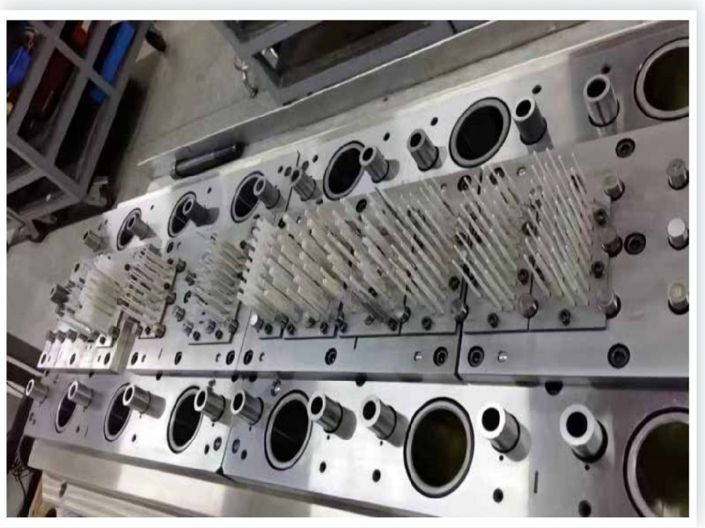
We can independently develop high-precision semiconductor stamping dies according to market needs, and our design concepts are industry-leading.
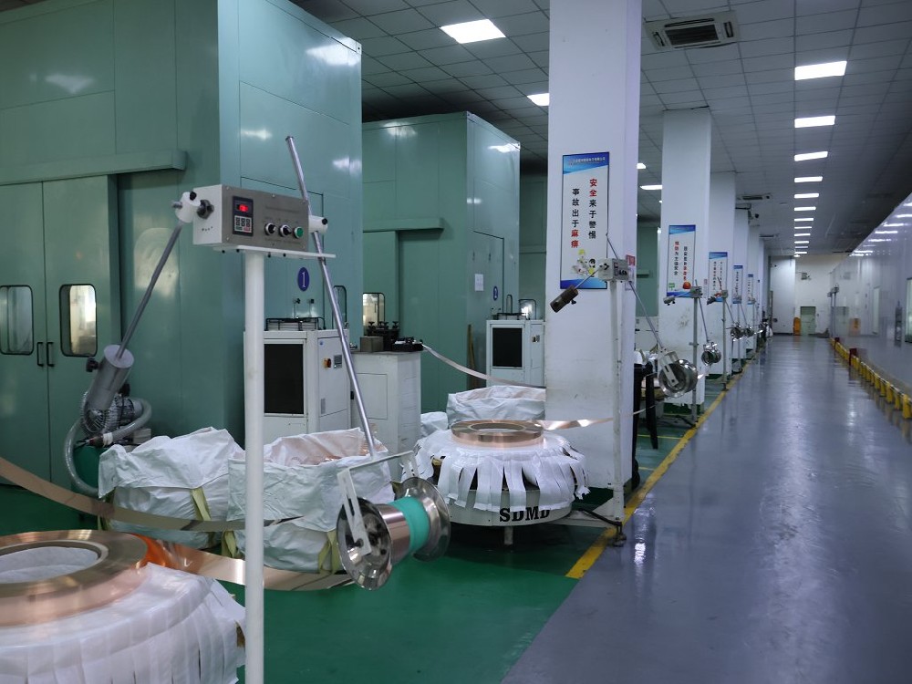
It has 70 high-speed stamping presses ranging from 40 to 125 tons, capable of stamping products of different specifications from 0.1 to 1.2 mm, with a monthly stamping capacity of 3.5 million K.
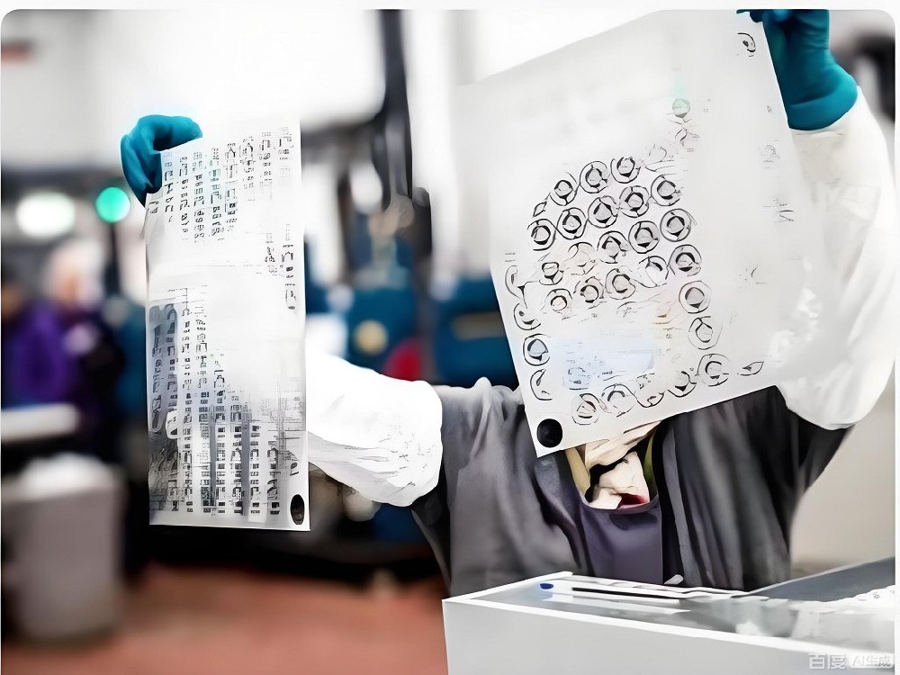
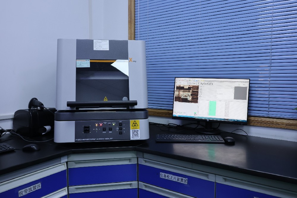
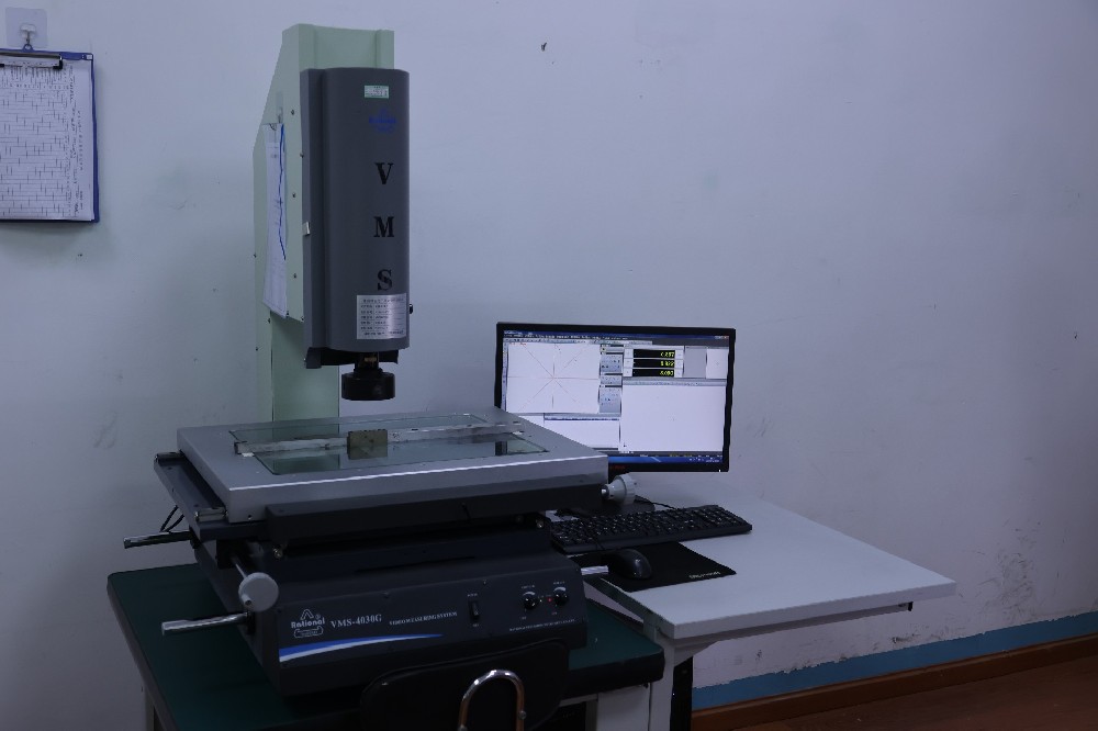
A precision etching production line has been established, with a processing capacity of over 500 pieces per hour and an accuracy of ≤0.02 mm.

The bending depth tolerance for materials with a thickness of 0.11~0.254mm is controlled within 0.015~0.025mm, and the bending depth tolerance for materials with a thickness of 0.40-1.2mm is controlled within 0.03~0.05mm. The monthly cutting capacity is 2.8 million kJ/kg.
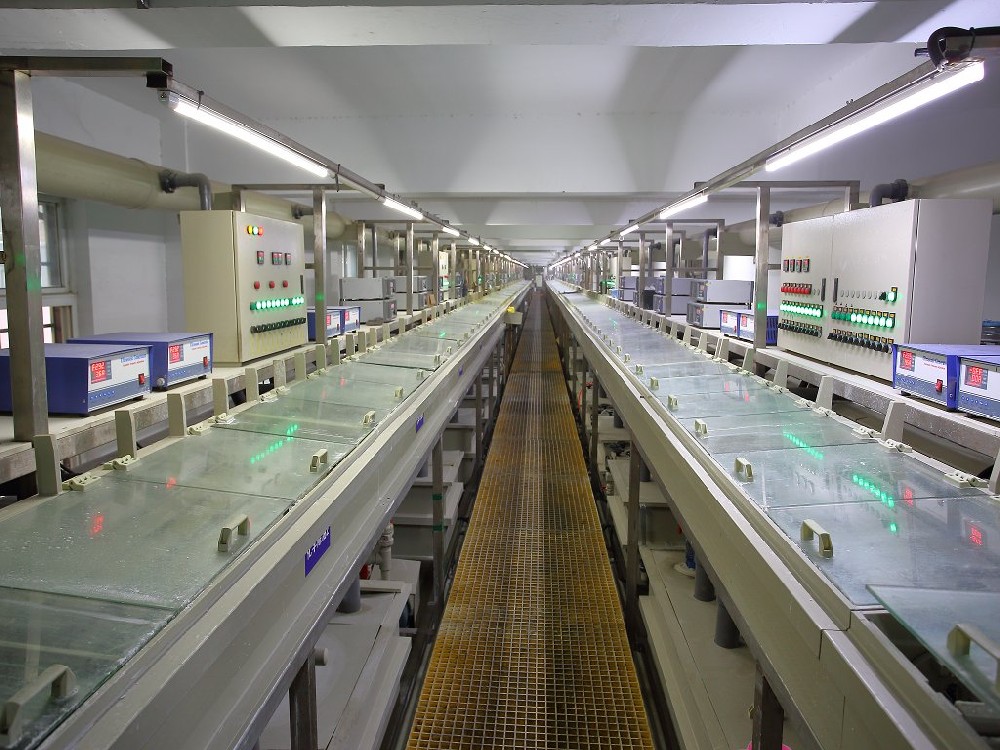
The fully automated electroplating line has 22 lines and 42 channels. The electroplating methods include full plating, ring plating, selective plating, strip plating, plate plating, and roughening. The monthly electroplating capacity is 3.5 million K.
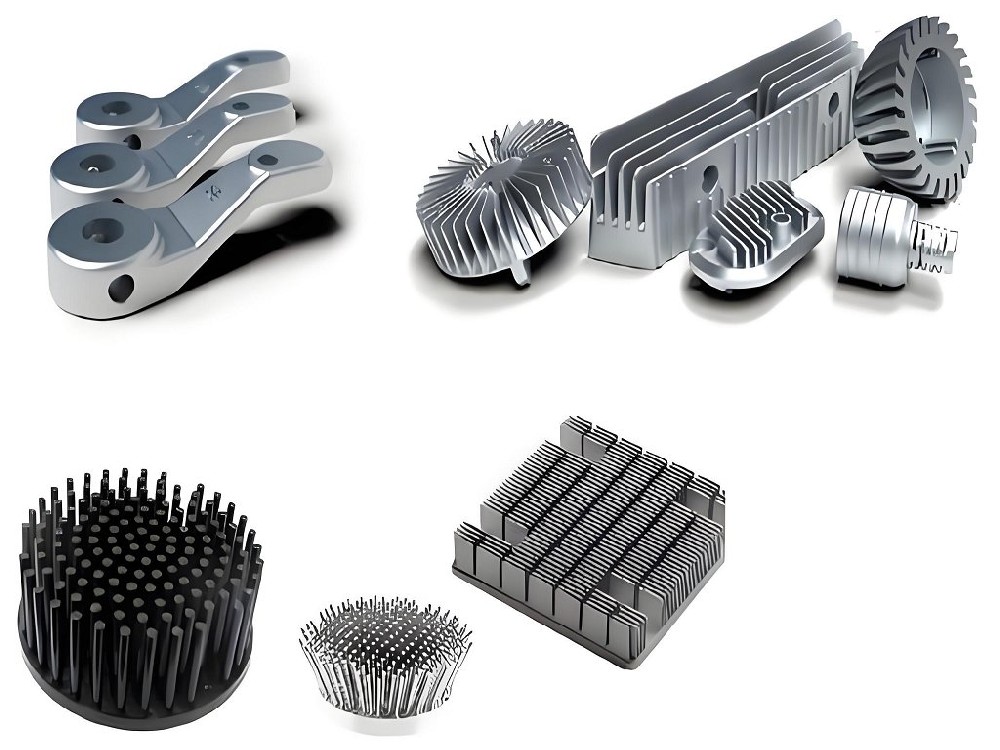
Cold forging equipment ranging from 800 tons to 5000 tons to meet the needs of different products.